| Place Of Origin: |
China ShenZhen |
Raw Material: |
FR4 |
| Layer Count: |
2-Layer |
Board Thickness: |
0.8-1.2mm |
| Copper Thickness: |
1oz |
Surface Finish: |
HASL Lead Free/HAL |
| Solder Mask: |
Blue |
Silkscreen: |
White |
| Min. Hole Size: |
0.25 |
Hole Wall Copper Thickness: |
≥20μm |
| Min. Trace Width/Spacing: |
0.075/0.075mm |
Packaging: |
Inner: Vacuum-packed In Soft Plastic Bales Outer: Cardboard Cartons With Double Straps |
| Application: |
Communication,automobile,cell,computer,medical |
Advantage: |
Competitive Price,Fast Delivery,OEM&ODM,Free Samples, |
| Special Requirements: |
Buried And Blind Via, Impedance Control, Via Plug, BGA Soldering And Gold Finger Are Acceptable |
|
|
| High Light: |
hdi circuit boards, universal pcb board |
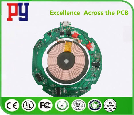
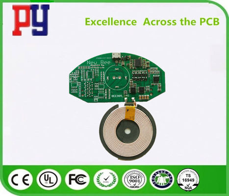
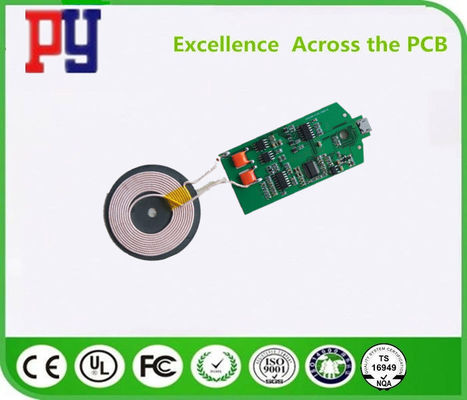
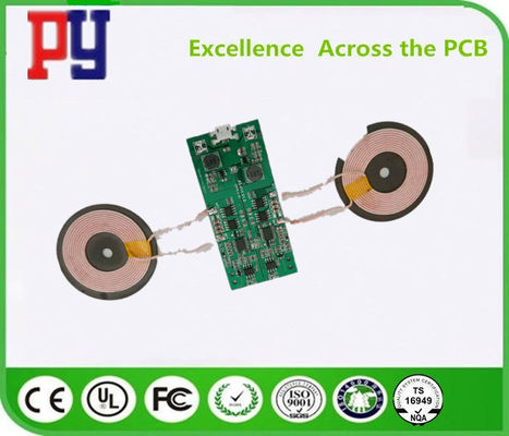
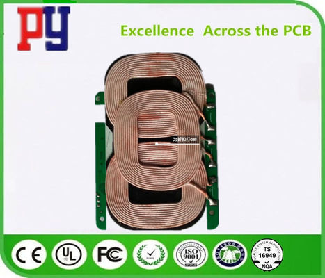
| Charging frequency |
100-200KHz |
| Output voltage |
5V |
| Output current |
500MA-1A |
| Output voltage |
19V |
| Power distance |
3-6mm |
| Electric energy transition |
≥70% |
| Receive electric current |
500-1000mAh adjustable |
| standard |
QI and MFI
|
1, the input charging voltage: DC5VC5%.
2, the output voltage: DC5V
3, the input charging current: 1000MA.
4, the output current: 1000mA.
5, Total quiescent current is less than 100uA.
6. Key Description; Press shows the power and go into standby then you can charge the internal battery or an external power supply equipment, long press 3 seconds on / off LED flashlight.
7, no-load output 20 seconds automatically shut down.
8, LED indication; charging 4 LED battery indicator, fully charged lights, rechargeable lights flashing, after fully charged 4 lights lit LED indicator first a light flashing the first two lights flash first three lights flash Chapter 4 lights flash, the battery were25% 25% 50% 50% 75% 75% 100%.
9, protection: over charge protection, over-discharge protection, short circuit protection.
10, suitable for most use DC5V charging mobile phones, cameras and other digital products
11, can be customized mobile power board and product development programs and
Advantages
a) FR-4 Single sided PCB with competitive price.
b) RoHS compliant and suitable for thermal reliability needs,and Lead free assemblies with a maximum reflow temperature of 260℃.
c) Engineering design prevents problems from occurring in pre production.
d) DDU Door to door shipment with competitive shipping cost. You don’t need to arrange anything after confirming the order. Just wait for your PCB delivery to your hand.
More Applications in Electronics
Battery Charger
PLC
Wireless
RF
Wifi Router
Design for Manufacture (1)
| Serial NO. |
Procedure |
Item |
Manufacturing capability |
| Large volume (S<100 m²) |
Middle volume (S<10 m²) |
Prototype(S<1m²) |
| |
| 1 |
Inner layer(18um, 35um, 70um etc are finished copper. If not mentioned copper, finished 1oz is the default value ) |
Min.isolation of layers |
0.1mm |
0.1mm |
0.06mm |
| 2 |
Min.track and spacing |
5/5mil(18um) |
4/4mil(18um) |
3/3.5mil(18um) |
| 3 |
5/5mil(35um) |
4/4mil(35um) |
3/4mil(35um) |
| 4 |
7/9mil(70um) |
6/8mil(70um) |
6/7mil(70um) |
| 5 |
9/11mil(105um) |
8/10mil(105um) |
8/9mil(105um) |
| 6 |
13/13mil(140um) |
12/12mil(140um) |
12/11mil(140um) |
| 7 |
Min.distance from drill to conductor |
4 Layer 10mil,6 layer 10mil,8-12 layer 12mil |
4 layer 8mil,6 layer 8mil,8-12 layer 10mil,14-20 layer 14mil,22-32 layer 18mil |
4 layer 6mil,6 layer 6mil,8-14 layer 8mil,16-22 layer 12mil,24-32 layer 14mil |
| 8 |
Min.width of annular ring on inner layer |
4 Layer 10mil(35um),≥6 Layer 14mil(35um) |
4 Layer 8mil(35um),≥6 layer 12mil(35um) |
4 Layer 6mil(35um),≥6 Layer 10mil(35um) |
| 9 |
Inner layer isolation ring width(Min) |
10mil (35um) |
8mil (35um) |
6mil (35um) |
| 10 |
Min.via pad diameter |
20mil (35um) |
16mil (35um) |
16mil (35um) |
| 11 |
Min. distance from board edge to conductor(no copper exposured)(inner layer) |
14 mil(35um) |
12 mil(35um)) |
8 mil(35um) |
| 12 |
Maximum copper weight(Inner layer and outer layer) |
3 OZ( 105 um ) |
4 OZ ( 140 um ) |
6 OZ( 210 um ) |
| 13 |
Core with different copper foil on both sides |
/ |
18/35,35/70 um |
18/35,35/70 u |
2oz (70um) Copper Double Sided HASL Lead Free PCB 1.6mm Thick Green Solder Mask Small Runs to Mass Production
Advantages
1. HASL has excellent wetting during component soldering and it can avoid copper corrosion
2. Save the cost of production: Production cost is one of the key points of our customers’ product competitiveness. Bicheng PCB have been striving to reduce its manufacturing cost from equipment introduce, worker training and technology improvement to increase their profitability. Customers are satisfied with our cost savings but without quality loss.
3. Great customer service
4. Customer complaint rate: <1%
5. Delivery on time: >98%
Applications
WiFi Card
Bluetooth Printer
Wireless Range Extender
Electric Motors
Tracking Device
Wireless Security System
Access Control
Data Logger
Intercom System
Surveillance System